
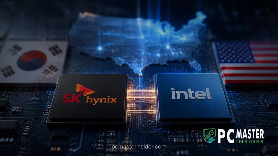
South Korean semiconductor leader SK Hynix is in preliminary discussions with Intel regarding a landmark agreement to manufacture memory chips inside the United States. The potential deal could mark SK Hynix's first memory wafer production facility on American soil, helping address severe global supply constraints driven by artificial intelligence infrastructure investments.
While negotiations remain in early stages, market reactions were immediate, with shares of both semiconductor companies rising on major exchanges following reports of the talks. The potential partnership arrives at a crucial juncture for both manufacturers as market pressures and geopolitical requirements reshape global chip production.
sk hynix intel memory manufacturing ohio fab
Negotiations between SK Hynix and Intel center on securing U.S.-based memory manufacturing capacity, with discussions exploring options to lease space at Intel's long-planned semiconductor complex in Ohio. The proposed arrangements aim to establish onshore production for high-demand memory products, offering a strategic pathway to mitigate global supply shortfalls and align with U.S. domestic manufacturing incentives.
SK Hynix and Intel U.S. Memory Manufacturing Negotiations
According to sources familiar with the preliminary talks, SK Hynix is exploring multiple avenues to establish wafer manufacturing capacity within the United States. Currently, neither SK Hynix nor rival Samsung Electronics produces raw memory wafers domestically in America, leaving U.S. data center operators heavily reliant on Asian imports for DRAM and NAND flash supplies.
While SK Hynix previously broke ground on a $4 billion advanced packaging facility in West Lafayette, Indiana, that site is dedicated purely to back-end packaging and testing of high-bandwidth memory (HBM). Under that model, processed DRAM wafers must still be shipped from fabs in South Korea before final assembly in Indiana. Partnering with Intel would allow SK Hynix to bring actual front-end wafer fabrication into the U.S. supply chain.
Addressing the preliminary reports, an SK Hynix spokesperson stated that the company is continually reviewing various options to strengthen its global competitiveness, including additional production sites, though no final decisions have been made. Intel similarly declined to comment on ongoing market rumors, reaffirming its commitment to developing its key domestic sites.
Potential Ohio Fab Lease and Cloud Joint Venture Scenarios
Industry sources highlight two primary operational structures currently on the negotiation table. The first scenario involves SK Hynix directly leasing factory floor space within Intel's multi-billion-dollar Ohio One campus, where completion of key production modules is projected for the late 2020s or early 2030s. This arrangement would allow SK Hynix to install its own specialized cleanroom tooling without bearing the immense capital expenditure required to build a greenfield facility from scratch.
The second option under evaluation is a joint venture structure combining SK Hynix, Intel, and major hyperscale cloud providers. Such a consortium would allow major cloud platforms to co-invest capital directly into dedicated memory lines, guaranteeing guaranteed memory allocations for their AI server fleets while offloading financial risk. Similar enterprise partnerships have become increasingly popular as data center operators seek to secure silicon supplies amid an intense memory stockpiles drop below 10 days across the technology sector.
Addressing the Global DRAM Shortage and Domestic Supply Chains
The rapid expansion of artificial intelligence workloads has created unprecedented demand for advanced memory architectures, particularly High Bandwidth Memory (HBM) and high-capacity DDR5 modules. Hardware vendors and enterprise cloud platforms continue to compete for limited allocation, driving up unit prices across server components. Meanwhile, PC component suppliers are adjusting to tight inventories, mirrored in retail movements where Framework retroactively cuts LPCAMM2 RAM prices as supply chains gradually stabilize.
Establishing domestic fabrication facilities would significantly shorten lead times for North American system integrators and hyperscalers. Furthermore, integrating localized memory fabrication alongside logic production aligns with broader hardware trends, where next-generation architectures like Intel Core Ultra 400 Nova Lake leaks highlight how cache size and memory access bandwidth are central to modern processor design.
Financial and Geopolitical Implications for Semiconductor Industry
For Intel, bringing in a major tenant or partner for its Ohio site could provide vital operational capital and improve capacity utilization for its long-term foundry strategy. Shares of Intel rose as much as 5.5% in early trading following news of the potential collaboration, reflecting investor optimism regarding shared capital burdens.
However, establishing wafer production in the U.S. presents steep financial and operational challenges for SK Hynix. Building and running advanced fabrication plants in North America incurs significantly higher labor, construction, and utility costs compared to Asian manufacturing hubs. Replicating complex supplier networks and localized raw material supply chains could elevate the total cost of U.S.-fabricated wafers.
The negotiations also carry strategic political weight. U.S. policy makers have aggressively pressured foreign chipmakers to build onshore capacity, threatening heightened tariffs on imported hardware for companies that fail to expand domestic footprints. Conversely, the South Korean government could voice objections over transferring cutting-edge memory IP or high-value manufacturing assets abroad, as Seoul actively supports a $520 billion domestic semiconductor initiative to retain its technological edge.
Next Steps and Regulatory Approval Hurdles
As discussions remain exploratory, any concrete deal will require months of formal structuring, financial auditing, and technical evaluation. The companies must decide whether production will focus on mainstream DRAM, NAND flash, or advanced HBM stacks, each requiring vastly different equipment and cleanroom configurations.
Any finalized agreement will also face stringent regulatory scrutiny. Authorities in both Washington and Seoul will evaluate the national security and economic impacts of domestic memory production. If approved, the collaboration between SK Hynix and Intel could re-shape the geographic distribution of global memory manufacturing over the coming decade.