
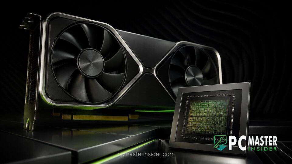
NVIDIA is reportedly preparing a secondary variant of its mid-range desktop graphics card powered by the larger GB203 GPU die. The move allows the semiconductor giant to repurpose partially defective silicon originally intended for higher-tier cards while maintaining consistent performance across the product line.
According to hardware industry insiders, the new configuration will feature heavily harvested GB203 chips that fail to meet the strict yield requirements for higher-tier products. This classic binning strategy enables NVIDIA to maintain steady supply chains without altering the baseline performance targets expected by retail consumers.
NVIDIA Prepares GB203 Die Transition for GeForce RTX 5070
Industry reports indicate that NVIDIA is expanding its silicon sourcing for the mid-range market by introducing a alternative physical revision for the desktop card. While the original release relies on the native GB205 processor, the upcoming nvidia geforce rtx 5070 gb203 die variant utilizes a scaled-down version of the larger physical package. Despite the underlying silicon shift, core hardware parameters such as CUDA core counts, memory capacity, and total graphics power are expected to remain completely identical to the standard retail model.
Silicon Specifications and Architectural Shifts
The standard GB205 processor features a physical die area of roughly 263 mm² housing approximately 31.1 billion transistors. By contrast, the flagship GB203 die measures 378 mm² with a massive transistor count of 45.6 billion, making it significantly larger and more expensive to manufacture per unit. To configure a GB203 processor for use in a lower tier, NVIDIA must disable roughly 43 percent of its active computing blocks and deactivate two of its eight 32-bit memory channels.
To match the baseline specification of the standard model, the reconfigured die will operate with 6,144 active CUDA cores alongside a 192-bit memory interface driving 12GB of GDDR7 VRAM. The power envelope will remain rated at a standard 250W TGP. Similar silicon repurposing strategies have appeared in past generations, as well as recent updates where lower-tier GPUs were adapted to run on cut-down mid-range chips to manage inventory levels.
Impact on Graphics Card Availability and Performance
For end users, the introduction of a larger chip inside a lower-tier product rarely translates to direct frame rate gains. Because clock speeds, memory bandwidth, and active execution units are strictly clamped to match original reference targets, real-world gaming performance should remain virtually indistinguishable between the two revisions.
However, running a heavily harvested die can occasionally yield minor secondary characteristics. A larger physical surface area distributes thermal dissipation over a wider section of the integrated heat spreader, which can sometimes result in marginally cooler operating temperatures under sustained heavy loads. Board partners may also need to adjust physical PCB designs to accommodate the slightly larger package layout and pin structure of the new processor.
This strategy offers clear supply advantages for the broader market. When wafer fabrication yields produce chips with minor localized flaws, disabling defective streaming multiprocessors enables manufacturers to salvage hardware that would otherwise be discarded. This approach maximizes factory yields from advanced foundry process nodes and helps maintain steady retail inventory levels during periods of high demand.
Driver Requirements and Market Context
To support the revised silicon, NVIDIA is expected to include updated device identification signatures in upcoming display drivers. Gamers who acquire boards featuring the secondary chip configuration will simply need to install the latest official display drivers to ensure full system stability and seamless operating system recognition.
This hardware transition arrives alongside broader software and hardware developments across the ecosystem. Gamers seeking granular control over modern features can explore updates like the NVIDIA App update with DLSS overrides or adjust performance parameters using tools designed to modify board behavior, as seen with utilities like mVolt bypassing VBIOS power limits. Concurrently, software innovations continue to evolve, with next-generation features such as NVIDIA DLSS 5 debut announcements expanding rendering capabilities across modern PC titles.
In summary, the reported silicon swap represents a practical supply chain management decision by NVIDIA. By converting partially disabled GB203 processors into functional mid-range offerings, the company optimizes silicon utilization while keeping performance metrics identical for everyday PC builders and gamers.