
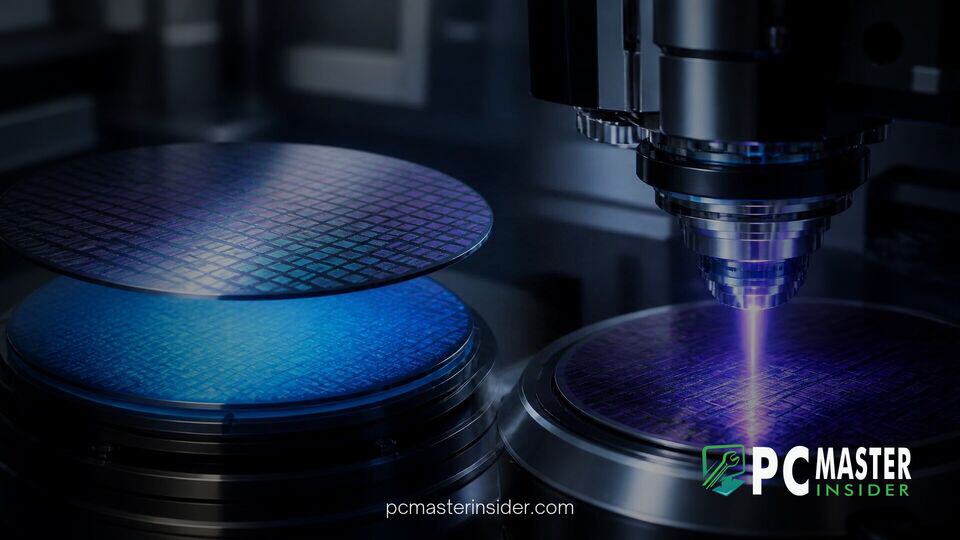
Micron Technology has detailed its long-term manufacturing strategy for next-generation dynamic random-access memory, announcing plans to integrate advanced wafer bonding and high-numerical-aperture extreme ultraviolet lithography into its upcoming process nodes. The strategy aims to extend planar memory scaling while systematically laying the groundwork for a eventual transition toward commercial 3D DRAM architectures.
During a recent technical briefing, executive leadership revealed that physical DRAM design is rapidly approaching fundamental physical boundaries. Rather than pursuing alternative transitional cell layouts that offer limited scaling life, Micron is focusing its capital research on process breakthroughs such as wafer-on-wafer bonding, High-NA EUV equipment, and stacked memory integrations.
micron high na euv wafer bonding dram
Micron's future process roadmap relies on combining wafer bonding and High-NA EUV lithography to advance DRAM density beyond current atomic constraints. By adopting these manufacturing tools alongside stacked 3D DRAM and vertical packaging concepts, the memory maker intends to deliver higher bandwidth and capacity without resorting to costly intermediate cell redesigns.
Micron Outlines Advanced DRAM Manufacturing Roadmap
The updated roadmap highlights a multi-step sequence designed to maintain performance progression across future memory generations. Micron is currently scaling its 1-gamma (1γ) node in high-volume production, which serves as the bedrock for immediate server and consumer offerings. Following this, the 1-delta (1δ) node is scheduled to enter volume manufacturing in the second half of 2027, yielding an estimated 25 percent improvement in bit density over its predecessor.
Moving beyond 1-delta, Micron will introduce its 1-epsilon (1ε) generation, which officially incorporates wafer bonding technology into the DRAM production process. The company will then transition to angstrom-class nodes, designated as zeta (ζÅ) and eta (ηÅ). These sub-10nm generations will integrate High-NA EUV scanners alongside novel dielectric materials to wring further spatial efficiency out of traditional 6F² cell geometry before 3D architectures take over fully.
Wafer Bonding and High-NA EUV Lithography Integration
Integrating wafer bonding allows memory designers to construct peripheral logic circuits on a separate silicon layer before bonding it directly to the memory array wafer. This separation optimizes silicon real estate, allowing peripheral control circuitry to be fabricated on standard CMOS processes without consuming valuable memory array footprint. Micron previously validated this architecture in its NAND flash division, where wafer-on-wafer bonding helped push 3D NAND cell counts well past 400 layers.
Complementing this architecture is High-NA EUV lithography. By utilizing an increased numerical aperture, High-NA scanners print significantly tighter critical dimensions in a single exposure. This reduces the need for complex multi-patterning techniques that drive up manufacturing defects and production costs. This equipment investment ensures that Micron DDR6 and LPDDR6 memory nodes can maintain tight tolerances as feature sizes approach sub-10nm scales.
Vertical HBM and On-Chip Edge Inference Memory
Alongside standard system memory, Micron unveiled new packaging concepts tailored specifically for high-density artificial intelligence compute. Among these is Vertical HBM (vHBM), a design where high-bandwidth memory stacks attach vertically on top of compute logic dies using hybrid copper-to-copper bonding rather than standard interposers. This setup dramatically shortens physical interconnect distances, reducing energy consumption per bit transferred.
Similarly, Micron detailed plans for vertical edge inference memory. By bonding memory arrays directly onto lightweight AI edge processors, hardware manufacturers can deliver low-latency local execution for agentic AI tasks. This approach arrives as demand for localized acceleration grows, driven by software ecosystems like Nvidia RTX Spark platform deployments and dedicated AI desktop acceleration.
Addressing Atomic Limits in Memory Density
A central reveal during the technical briefing was Micron's decision to bypass 4F² cell designs. While industry peers like CXMT have pursued 4F2 DRAM designs for DDR5 server memory, Micron executives argued that 4F² structures present serious scaling roadblocks without yielding true density advantages.
"DRAM is nearing atomic limits at this point," said Scott DeBoer, president and chief technology and products officer at Micron. "Although we have confidence in several more planar nodes, we are very focused on making sure that we introduce 3D DRAM at the optimal time from a cost and performance point of view."
DeBoer clarified that capacitor pitch, rather than transistor geometry alone, dictates true DRAM density. Because 4F² layout transitions do not resolve underlying capacitor scaling limits, Micron concluded that investing heavily in 4F² yields diminishing returns compared to mastering High-NA EUV and 3D DRAM fabrication.
Industry Impact and Next-Generation PC Hardware
Micron's strategic focus comes at a pivotal moment for the broader hardware sector. Over the past year, supply restrictions and high manufacturing costs have impacted global hardware markets. System integrators and consumer markets have already faced elevated memory costs, causing global PC shipments to fall significantly in recent quarters.
Furthermore, surging demand for AI server clusters has tightened total DRAM wafer allocation worldwide. Extreme pricing pressures have even led notable technology executives like Elon Musk to criticize memory pricing across the supply chain, even while commending Micron for its long-term manufacturing vision.
By focusing its capital expenditures directly on High-NA EUV, advanced wafer bonding, and direct 3D memory scaling, Micron aims to stabilize production efficiency and lower cost-per-bit metrics over the next decade. If successful, these process innovations will ensure a steady supply of high-density memory required for future server architectures, consumer platforms, and advanced AI hardware.