
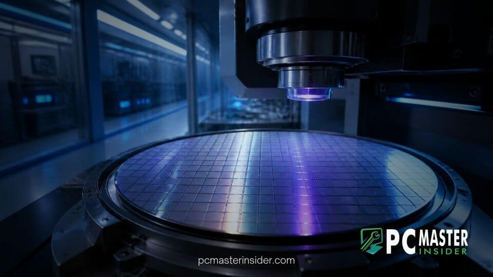
Intel Foundry and ASML have announced a significant milestone in advanced semiconductor manufacturing, revealing that over one million 300 mm wafers have been processed using High-Numerical Aperture (High-NA) Extreme Ultraviolet (EUV) lithography systems. The milestone encompasses early tool certification, research and development, and high-volume commercial production for select layers of Intel Core Ultra Series 3 processors, code-named Panther Lake.
The announcement underscores Intel's strategy of early adoption for ASML's most complex scanner technology. By integrating High-NA EUV into operational fab lines ahead of industry competitors, the company aims to validate process maturity and secure commercial manufacturing efficiency for its advanced node roadmap.
Intel Foundry Reaches 1 Million High-NA EUV Wafer Milestone
Intel Foundry confirmed that its cumulative volume of processed High-NA EUV wafers has reached seven figures across its development and manufacturing network. The milestone reflects operations across multiple scanner installations, including early-generation TWINSCAN EXE:5000 tools and the newer high-throughput TWINSCAN EXE:5200B scanners operating at Intel's primary R&D facilities in Oregon.
This achievement highlights the rapid operational ramp-up since Intel installed the world's first commercial High-NA EUV scanner in early 2024. While initial deployment targeted testing for the upcoming Intel 14A node, engineers successfully extended High-NA exposure to specific critical layers on the commercial Intel 18A process node. As a result, commercial silicon for consumer platforms is actively running through High-NA scanners alongside internal process development wafers.
Panther Lake Production and 18A Node Progress
A key driver of recent wafer throughput is the commercial production of Intel's Panther Lake processor family. Intel Foundry is applying High-NA exposure to select dense metal and transistor gate layers on a subset of Panther Lake SKUs. By replacing complex multi-patterning runs on standard low-NA (0.33 NA) EUV equipment with single-exposure High-NA steps, Intel has reduced mask counts, lowered defect rates, and shortened fab cycle times.
According to joint performance reports from Intel and ASML, key operational metrics such as tool availability, layer overlay precision, and wafer throughput meet or exceed target expectations. Furthermore, silicon layers patterned with 0.55 NA systems have matched or surpassed the electrical performance standards established on standard 0.33 NA EUV lines. Technical progress on these fabrication techniques closely aligns with architecture developments seen across products like Intel Wildcat Lake architecture, which also targets efficient node design.
Technical Breakthroughs with ASML High-NA Lithography
The transition from conventional 0.33 NA EUV to 0.55 High-NA EUV represents one of the largest optical engineering transitions in modern chip manufacturing. High-NA optics allow tighter focus of 13.5 nm wavelength ultraviolet light, enabling single-print feature resolution down to 8 nm. This capability allows chipmakers to print sub-2nm transistor features without resorting to expensive triple or quadruple patterning schemes.
However, the anamorphic optical design of High-NA systems introduces a half-field exposure limit, reducing the maximum exposure area on a standard photomask to 26 mm by 16.5 mm. This restriction requires chip designers to either adapt layout floor plans or implement reticle stitching to assemble large dies across multiple exposure fields.
Overcoming Photomask Stitching Constraints
To address the half-field challenge without delaying customer adoption, Intel Foundry introduced process design kits (PDKs) that enable external foundry clients to floor-plan within current 6-inch reticle formats. For larger dies, Intel implemented reticle stitching techniques that seamlessly join two exposure fields during the lithography step without compromising yield.
Concurrently, Intel Foundry and ASML are leading a broader industry initiative to pioneer larger 6x12-inch photomask standards. Transitioning to double-length reticles will eventually eliminate reticle stitching requirements for enterprise-grade processors and high-performance accelerators, such as those powering modern data centers. Industry ecosystem partners, including mask shops, electronic design automation (EDA) vendors, and materials suppliers, are currently working on infrastructure for this future standard.
Industry Impact and Future Node Roadmap
Intel's focus on High-NA EUV deployment marks a clear divergence in strategy compared to competing foundry operators. Key competitors such as TSMC and Samsung have largely opted to maximize existing 0.33 NA EUV multi-patterning setups for their initial 2nm-class nodes, citing the high capital cost of High-NA tools. TSMC plans to introduce High-NA equipment closer to its sub-2nm nodes later in the decade, while Samsung is targeting adoption around 2028 to 2030.
By absorbing the early adoption learning curve, Intel Foundry aims to establish a lead in defect reduction and yield optimization. This operational experience is critical as Intel prepares its upcoming 14A process node for volume manufacturing, which will rely more heavily on High-NA lithography across multiple primary layers. Intel's aggressive manufacturing roadmap complements its broader silicon portfolio, including large-scale server chips like Intel Diamond Rapids Xeon CPUs and specialized accelerators like Intel Crescent Island AI accelerator units.
ASML Chief Executive Officer Christophe Fouquet commended Intel's leadership in advancing the High-NA ecosystem from initial installation through high-volume logic manufacturing. As external foundry customers evaluate advanced nodes for next-generation products, Intel's milestone of one million processed wafers provides practical evidence that High-NA lithography has successfully transitioned from experimental labs to high-volume manufacturing.