Fujitsu presented detailed architectural specifications for its upcoming Monaka data center processor during the Hot Chips 2026 symposium. The 144-core Arm-based server CPU combines 2nm compute dies with a dedicated 3D-stacked 5nm SRAM cache tier to boost energy efficiency across enterprise and artificial intelligence infrastructure.
Designed as the successor to the A64FX processor that powered Japan's Fugaku supercomputer, Monaka shifts Fujitsu's target from specialized supercomputing to mainstream data centers and sovereign AI deployments. By utilizing vertical chiplet integration, Fujitsu aims to deliver twice the performance and energy efficiency of competing server platforms while keeping manufacturing costs under control.
Fujitsu Monaka 144 Core Server CPU Hot Chips Architecture Breakdown
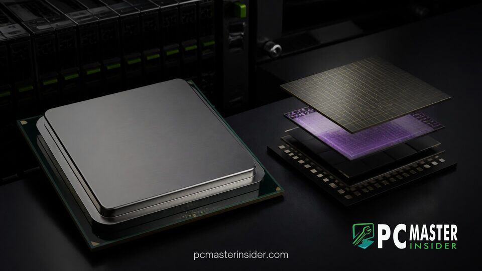
The Monaka processor architecture relies on a multi-die design split across three distinct silicon tiers. The primary compute layer consists of four 36-core CPU chiplets fabricated on TSMC's 2nm (N2P) process node. These compute dies are stacked face-to-face via direct hybrid copper bonding directly on top of a 5nm SRAM cache die, which houses the processor's entire last-level cache. Underneath, an I/O die fabricated on a 5nm process handles system connectivity across a silicon interposer.
During the Hot Chips 2026 presentation, Fujitsu lead architect Ryohei Okazaki highlighted that 2nm silicon accounts for less than 30 percent of the total die area in the Monaka package. By reserving the expensive 2nm node strictly for core execution logic while keeping SRAM and I/O components on mature 5nm processes, Fujitsu optimizes silicon yield and lowers production costs. Stacking the compute dies on top of the cache layer also places the highest-power logic closest to heat dissipation solutions.
Similar advancements in 3D silicon packaging and chiplet interconnects were showcased across the conference, reflecting industry trends seen in Arm Details AGI Server Processor with Dual 70-Core Chiplets at Hot Chips 2026 and Intel Unveils Diamond Rapids Xeon CPUs with Up to 256 P-Cores at Hot Chips.
SVE2 Vector Engines and Power Configurations
Fujitsu built Monaka around the Armv9.3-A instruction set architecture, incorporating dual 256-bit Scalable Vector Extension 2 (SVE2) execution units per core. This design choice contrasts with the 512-bit vector units on the older A64FX processor, trading raw vector width for improved software compatibility and better power scaling across general cloud workloads.
The chip supports dual-socket server nodes, allowing system builders to deploy up to 288 physical Arm cores within a single 2U rack mount chassis. Platform connectivity includes 12 channels of DDR5 memory alongside PCIe 6.0 lanes integrated with CXL 3.0 support for memory expansion.
Fujitsu confirmed two distinct power configurations for Monaka server implementations:
- 350W Air-Cooled Variant: Operating at a 2.1 GHz base clock, tailored for standard enterprise rack environments.
- 500W Liquid-Cooled Variant: Operating at a 2.9 GHz base clock, optimized for high-density compute clusters and demanding AI workloads.
Focus on Green Data Centers and Agentic AI Workloads
Fujitsu emphasized that Monaka addresses growing power constraints inside modern hyperscale facilities. As cloud providers grapple with soaring electricity demands driven by AI inference and agentic orchestration tasks, ultra-low-voltage processor architectures offer an alternative to power-hungry GPU clusters.
Rather than acting purely as control units for external accelerators, modern data center CPUs are increasingly tasked with complex data pipelines, pre-processing, and agentic AI workflows. Fujitsu's architecture allows execution at sub-nominal operating voltages without sacrificing single-thread latency, reducing overall thermal footprints.
The push for vertical memory stacking in data center chips comes as the broader semiconductor market responds to rising memory costs and capacity limitations. These supply dynamics match trends detailed in Intel CEO Hints at Return to Memory Business and CPU Memory Stacking and Memory Chipmakers Sell Out 2027 DRAM Supply as AI Demand Dominates Capacity.
Availability Timeline and Ecosystem Strategy
Development of the Monaka processor has been partially subsidized by Japan's New Energy and Industrial Technology Development Organization (NEDO). Fujitsu confirmed that early evaluation silicon and engineering samples are currently in the hands of key hardware partners.
Volume commercial shipments for Monaka-based servers are scheduled to begin in 2027. Beyond Monaka, Fujitsu revealed long-term roadmap plans for a successor chip codenamed Monaka-X, targeted for a 2029 release on a 1.4nm process node.
By leveraging open standards, 3D chiplet integration, and Arm's software ecosystem, Fujitsu is positioning Monaka as a key player in the next generation of energy-efficient cloud and enterprise server hardware.