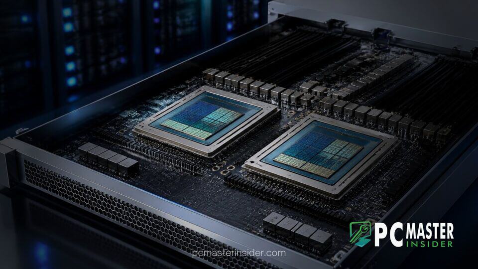
At the Hot Chips 2026 conference, Arm detailed its latest server processor architecture designed specifically to address the compute demands of artificial general intelligence (AGI) and large-scale data center deployment. The presentation highlighted a dual-chiplet design pairing two 70-core compute tiles, providing a total of 140 high-performance cores on a single multi-chip package.
Engineered for hyper-scale cloud environments, the architecture focuses on breaking through processing bottlenecks while optimizing energy efficiency across massive clusters. By combining high-density custom cores with high-speed die-to-die interconnects, Arm aims to offer enterprise data centers an alternative to traditional monolithic server processors.
Arm AGI Server CPU Hot Chips 2026 Disclosure Details
During its presentation, Arm revealed that the flagship design centers on two identical 70-core compute chiplets integrated onto a unified substrate. The dual-chiplet configuration delivers 140 instruction-execution threads without relying on traditional simultaneous multithreading, ensuring predictable latency across intensive compute tasks. Each compute die is linked via a low-latency, high-bandwidth interconnect that treats the combined cores as a coherent uniform memory access (NUMA) domain for simplified software deployment.
This architectural shift aligns with industry-wide efforts to move beyond monolithic silicon manufacturing. As top-tier chip manufacturers like Intel highlight multi-core scalability in enterprise platforms like Intel Diamond Rapids Xeon CPUs featuring high P-core counts, Arm is leveraging chiplet modularity to deliver customized silicon for hyperscalers while keeping production yields high.
Arm Outlines Dual-Chiplet Architecture for Next-Gen Data Centers
The foundation of Arm's new server architecture relies on a decoupled design that isolates compute-heavy logic from input/output and memory controllers. By splitting the processor into distinct functional units, Arm allows data center operators and silicon partners to tailor the I/O configurations to specific cluster requirements without redesigning the core compute tiles.
This chiplet strategy aims directly at scalable cloud deployments where AI model training and inference require massive parallel compute. The architecture supports multi-socket configurations, allowing system builders to scale up thread density per server rack while maintaining tight energy budgets.
Key Specifications and N3P Manufacturing Process
The 70-core compute chiplets are manufactured using TSMC's advanced N3P 3nm-class process node, providing significant improvements in logic density and power efficiency compared to previous generation server cores. Operating clock frequencies are targeted to balance high single-thread execution speed with optimal thermal envelopes in high-density server racks.
Key technical highlights disclosed at the conference include:
- Total Core Count: 140 custom Neoverse-based cores across two 70-core compute tiles.
- Process Technology: TSMC N3P process node for compute tiles.
- Cache Hierarchy: Expanded private L2 caches per core with a massive shared L3 distributed cache across the interconnect fabric.
- Instruction Set: Native support for SVE2 (Scalable Vector Extension) and SME2 (Scalable Matrix Extension) to accelerate matrix math operations common in neural networks.
High-Bandwidth Interconnect and Memory Controller Features
To feed 140 cores without starving execution units, Arm has integrated a next-generation die-to-die interconnect capable of multiple terabytes per second in bi-directional bandwidth. The interconnect utilizes advanced packaging technology to minimize physical distance, reducing latency to near-monolithic levels.
The system supports multi-channel DDR5 memory controllers along with direct integration options for High Bandwidth Memory (HBM). This flexible memory subsystem is vital during a period when the enterprise market is navigating high component costs, as reflected in wider industry trends where enterprise DDR5 memory prices have surged due to global data center demands. Furthermore, with market analysts noting that Nvidia AI server prices face upward pressure from memory supply constraints, Arm's flexible controller architecture gives hardware integrators options to balance high-speed HBM with standard DDR5 channels.
Impact on AI Workloads and High-Performance Computing
Arm designed the dual 70-core processor to act as both a primary host processor for large-scale AI accelerators and an independent engine for complex inferencing tasks. By embedding matrix acceleration directly into every core, the platform can handle medium-sized AI models without offloading tasks to external discrete GPUs.
Industry analysts at Hot Chips noted that Arm's focus on matrix performance per watt positions the chiplet architecture well for AGI pipelines, which require continuous contextual processing and massive data throughput. The capability to execute vector and matrix operations natively on the host CPU reduces data transfer overhead across PCI Express buses, improving overall system responsiveness in real-time language modeling and automated reasoning workloads.
Commercial Availability and Deployment Timeline
Arm confirmed that production silicon based on the dual 70-core architecture is scheduled to reach lead hyperscale partners for initial sampling in late 2026, with broader commercial availability expected in 2027. Major cloud service providers are anticipated to integrate the IP into custom silicon designs tailored for their own cloud infrastructure.
As AI workload demands continue to redefine server hardware requirements, Arm's modular, chiplet-based approach offers a highly efficient blueprint for future data center computing. By combining high core density, flexible memory options, and specialized vector processing, the platform represents a significant step forward in meeting the compute requirements of next-generation artificial intelligence platforms.