Intel Chief Executive Officer Lip-Bu Tan has signaled a potential strategic shift that could see the semiconductor pioneer re-engage with the memory market. Speaking on industry developments, Tan highlighted that advanced packaging technologies and 3D CPU-memory stacking have converted memory from a low-margin commodity into a vital strategic asset for modern computing workloads.
The CEO revealed that exploring next-generation memory architectures and tight integration strategies has become a key internal focus for the company. While formal product rollouts remain undisclosed, Intel has already made notable moves, including hiring veteran industry leadership to oversee advanced packaging initiatives as AI computing demands higher memory bandwidth and efficiency.
Intel Explores Strategic Re-Entry into Memory Chip Manufacturing
For decades, Intel was closely associated with compute logic, having famously exited the dynamic random-access memory (DRAM) business in the mid-1980s to concentrate on microprocessors. Later, the company divested its NAND flash memory business to SK Hynix. However, the rise of artificial intelligence, high-performance computing (HPC), and persistent global memory constraints have reshaped the economics of the memory market.
Tan noted during a recent discussion on semiconductor trends that memory was historically viewed as a commodity with volatile margins, but technological shifts have altered that narrative. With AI systems facing severe bandwidth and power bottlenecks, the memory layer now dictates system performance as much as the central processing unit itself. Consequently, developing custom memory architectures and manufacturing methods offers new opportunities for differentiation.
To support this potential pivot, Intel has brought in experienced memory talent, including former SK Hynix executive Seok-Hee Lee, to strengthen its advanced packaging and foundry operations. While Tan clarified that Intel is not ready to disclose specific manufacturing commitments, the talent acquisition demonstrates a clear commitment to exploring novel memory topologies.
Next-Generation CPU and Memory Stacking Architectures
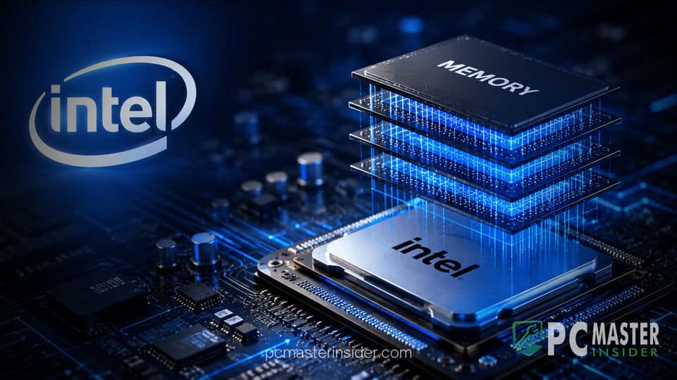
At the center of Intel's emerging direction is the strategic integration of memory directly alongside or on top of processing units. Advanced 3D packaging technologies, such as Intel's proprietary Foveros platform, allow different silicon dies to be stacked vertically rather than placed side-by-side on a printed circuit board or silicon interposer.
By placing memory dies directly over the compute die, interconnect distances are drastically reduced. This vertical stacking yields three crucial benefits:
- Reduced Latency: Electrical signals travel significantly shorter distances between the processor cores and memory cells, accelerating data access times.
- Higher Bandwidth: Microscopic vertical interconnects allow thousands of simultaneous connections, dramatically increasing interconnect density compared to traditional traces.
- Improved Energy Efficiency: Pushing data across shorter physical distances consumes far less power, helping control thermal output in dense server environments.
Engineers across the semiconductor landscape recognize that standard off-chip memory buses struggle to keep pace with multi-core CPUs and AI accelerators. Stacking memory directly on compute dies offers a viable path to eliminate interconnect bottlenecks without vastly expanding the physical footprint of the processor package.
Intel CPU Memory Stacking Strategy to Tackle AI Bottlenecks
The primary driver behind the Intel CPU memory stacking strategy is the rapidly evolving architecture of artificial intelligence infrastructure. Large language models and complex deep learning workloads require massive datasets to pass between memory arrays and processing units continuously. When memory bus speed fails to match computing capability, high-performance chips spend valuable cycles waiting for data delivery.
Intel aims to address this memory wall by combining its advanced packaging technologies with customized memory layers. Rather than relying solely on standard high-bandwidth memory (HBM) modules connected via interposers, direct vertical integration could streamline the supply chain and deliver superior bandwidth density. This approach aligns with Intel's broader foundry ambitions, where advanced packaging services are offered both for internal chip designs and external foundry customers.
However, 3D stacking presents notable engineering hurdles, particularly regarding thermal management and manufacturing yields. Stacking hot DRAM or custom memory layers directly on top of a high-power CPU logic die creates significant heat dissipation challenges. Managing thermal spread without throttling processor performance requires specialized thermal interface materials and complex physical designs. Furthermore, stacking multiple functional dies together increases the risk of lower overall yield if a single layer exhibits defects.
Market Context and Strategic Impact on Semiconductor Industry
Intel's renewed focus on memory and vertical integration comes during a critical transition period for the company. As the business continues to expand its foundry services and invest heavily in next-generation process nodes, offering integrated compute-plus-memory solutions provides a distinct competitive edge.
Rivals in the industry have also pursued vertical integration and advanced packaging to boost processing capabilities. Competitors like AMD have successfully commercialized 3D stacked cache to improve gaming and server performance, while TSMC and Samsung continue to expand their own 3D packaging ecosystems. By targeting deep CPU-memory convergence, Intel seeks to position itself at the forefront of post-reticle chip architecture.
Financial analysts note that while re-entering full-scale DRAM commodity manufacturing from scratch would require immense capital expenditure, focusing on specialized, stacked memory solutions leverages Intel's existing strengths in packaging and silicon design. Proceeds from recent capital raises and strategic partnerships are expected to support ongoing research and foundry infrastructure tailored for these advanced architectures.
In summary, Intel's exploration of CPU-memory stacking reflects a broader transformation in how high-performance processors are built. By treating memory design and packaging as central elements of processor architecture rather than separate peripheral components, Intel aims to solve critical data bottlenecks for the next generation of computing systems.