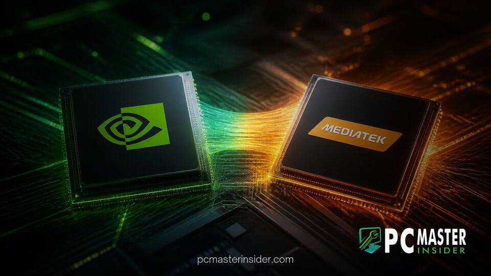
NVIDIA has officially disclosed a strategic $3.5 billion investment in MediaTek to co-develop custom artificial intelligence computing platforms and expand its proprietary interconnect standards. The financial agreement, structured via convertible bonds, cements a deep technical partnership aimed at accelerating custom silicon design from edge devices to enterprise data centers.
By leveraging MediaTek's ultra-low-power system-on-chip expertise alongside NVIDIA's dominant graphics and enterprise AI architecture, the two semiconductor giants plan to address rising global demand for scalable inference and training silicon. The collaboration marks one of NVIDIA's largest direct investments in an external chip design house to date.
NVIDIA MediaTek $3.5 Billion Investment in AI Chips Disclosed
Under the newly disclosed regulatory filings, NVIDIA's $3.5 billion capital commitment directly funds joint engineering initiatives focused on co-designing specialized hardware accelerators. The partnership utilizes MediaTek's established ties with advanced manufacturing foundries and its extensive portfolio of energy-efficient mobile designs. In return, NVIDIA secures dedicated capacity for custom silicon projects tailored for enterprise clients demanding modular AI solutions.
Industry analysts view this capital allocation as a proactive step to diversify silicon manufacturing routes and broaden the reach of NVIDIA's architecture beyond traditional standalone graphics processors. By co-developing silicon directly with MediaTek, NVIDIA aims to lower latency and power consumption in hybrid computing environments that combine mobile edge systems with cloud infrastructure.
Details of NVIDIA’s $3.5 Billion Convertible Bond Investment in MediaTek
The investment structure centers on convertible bond instruments issued by MediaTek, allowing NVIDIA to convert its debt holding into equity under predefined market conditions. This structure provides MediaTek with immediate, non-dilutive balance sheet strength to scale up specialized research and development facilities without compromising existing shareholder structures.
Financial details reveal that the proceeds are strictly earmarked for joint venture R&D projects, including high-density packaging, advanced node design tools, and customized software development kits (SDKs). The funding structure ensures long-term alignment between both firms, binding their hardware engineering roadmaps together across multiple product generations.
Building Custom XPUs and NVLink Fusion Rack-Scale Infrastructure
A primary technical pillar of the agreement is the joint creation of customized application-specific integrated circuits, broadly referred to as custom XPUs. These accelerators will combine MediaTek's energy-efficient compute blocks with custom NVIDIA tensor engines. Furthermore, the collaboration brings NVIDIA's high-speed NVLink interconnect topology to MediaTek's custom chiplet designs.
Integrating NVLink technology allows MediaTek-designed accelerators to communicate directly with NVIDIA GPUs and enterprise host CPUs at ultra-high bandwidths with minimal latency. This capability is crucial for modular rack-scale architectures, where multi-chip modules must operate as a unified computing system. The initiative complements existing industry efforts, such as NVIDIA's specialized rack architectures detailed at Hot Chips, by providing flexible building blocks for data centers requiring tailored computing topologies.
Expanding AI Computing Platforms from Edge Devices to Cloud Factories
The strategic alliance reaches far beyond enterprise server racks, aiming to bridge the functional gap between edge devices and massive AI cloud centers. MediaTek has long held a dominant position in smart TVs, handheld devices, automotive infotainment, and mobile platforms. Infusing these platforms with NVIDIA's hardware architecture and CUDA software ecosystem enables edge hardware to run complex neural networks locally while maintaining seamless compatibility with cloud-hosted models.
This edge-to-cloud integration complements other major industry memory and compute shifts aimed at on-device performance, similar to how Samsung's smart LPDDR5X-PIM memory brings processing-in-memory logic to mobile platforms. By optimizing software runtimes across both mobile chips and data center accelerators, developers can train models in the cloud and deploy them directly onto MediaTek-powered edge systems without re-architecting their software pipelines.
Strategic Implications for the Global AI Semiconductor Industry
The alliance reshapes competitive dynamics within the global semiconductor supply chain. For MediaTek, partnering with the world's leading AI hardware vendor elevates its standing in the high-margin enterprise data center sector, complementing its traditional volume business in consumer electronics. The company gains access to high-bandwidth interconnect IP and enterprise software stacks that would otherwise take years to develop independently.
For NVIDIA, working with MediaTek mitigates rising complexity costs across advanced process nodes. As the industry transitions to multi-chiplet packaging and custom node configurations, collaborating with an experienced chiplet design partner allows NVIDIA to service niche enterprise requests without diverting internal resources away from flagship architectures. This approach aligns with broader market trends where silicon designers share packaging technologies, reminiscent of how Intel leverages open UCIe standards for multi-die CPUs and Arm utilizes dual 70-core chiplet architectures for scale-out clusters.
Executive leadership from both organizations highlighted the transformative nature of the agreement during joint disclosures. "Connecting MediaTek's leadership in low-power System-on-Chip designs with NVIDIA's unmatched computing scale creates an unprecedented opportunity," noted semiconductor research analysts following the disclosure. "It effectively establishes a unified architecture spanning from battery-powered edge silicon to megawatt-scale enterprise factories."
Projected Deployment Timeline and Market Impact
The initial wave of co-developed products arising from the $3.5 billion investment is expected to tape out over the next 18 to 24 months, with early commercial sampling targeted for enterprise testing phases shortly thereafter. Initial deployment phases will prioritize custom automotive cockpit chips and high-efficiency inference modules designed for edge data centers.
Subsequent rollouts will introduce full NVLink-enabled XPU modules intended for large-scale data center integrations, offering hyperscalers an alternative to fully custom internal silicon efforts. As cloud operators continue to balance power constraints against compute demands, high-efficiency custom chiplets built on proven mobile IP will play an increasingly vital role.
NVIDIA's $3.5 billion investment in MediaTek establishes a powerful framework for the future of custom silicon design. By combining financial backing with shared intellectual property, both companies are well-positioned to drive the next phase of global AI infrastructure expansion, uniting edge efficiency with cloud-scale performance.