
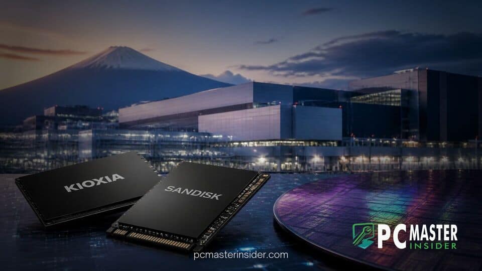
Kioxia Corporation and Sandisk have unveiled a joint capital expenditure plan totaling nearly $31 billion to dramatically scale up flash memory manufacturing in Japan. The multiyear investment program aims to expand cleanroom capacity and deploy cutting-edge 3D NAND fabrication tools across their shared manufacturing sites.
This joint effort arrives as global demand for solid-state storage surges, driven by hyperscale cloud expansion and intensive artificial intelligence training clusters. By ramping up localized domestic output, the partnership seeks to stabilize worldwide supply chains while securing a central role in high-density enterprise storage.
Kioxia Sandisk Japan Flash Memory Investment
Under the dynamic new agreement, the joint venture will allocate significant resources toward building out next-generation manufacturing lines. The multi-trillion yen commitment, equivalent to roughly $31 billion over the operational roadmap, covers cleanroom construction, advanced EUV lithography integration, and high-aspect-ratio etching equipment. This massive joint venture endeavor represents one of the largest single semiconductor manufacturing updates in Japan's history, strengthening the structural alliance between Kioxia and Western Digital's Sandisk brand.
Kioxia and Sandisk Announce $31 Billion Joint Expansion
The joint capital expenditure agreement marks a renewed era of collaboration between the long-time memory partners. The capital commitment will be deployed incrementally over several fiscal years, funding both infrastructure expansion and advanced research and development. Both companies plan to leverage the investment to transition their primary production pipelines toward highly dense, stacked 3D NAND architectures featuring upward of 200 to 300 vertical layers.
Industry analysts note that this aggressive investment schedule highlights the critical need for memory manufacturers to keep pace with enterprise demand. As AI clusters expand worldwide, reliable high-speed storage has become as vital as raw compute power. Earlier market assessments revealed that memory chips are projected to reach 60 percent of global semiconductor market revenue, underscoring the massive financial incentive behind multi-billion-dollar fabrication projects.
Funding Allocation Across Yokkaichi and Kitakami Facilities
The capital expenditure strategy centers around two main production hubs in Japan: the expansive Yokkaichi plant in Mie Prefecture and the modern Kitakami plant in Iwate Prefecture. A significant portion of the immediate funding will go toward completing specialized cleanrooms at Kitakami's Fab 2 facility, alongside equipment installations at Yokkaichi's Fab 7.
By spreading the capital allocation across both locations, the joint venture ensures operational redundancy while optimizing logistics. The expansion plans include upgrading existing fabrication tools to support BiCS FLASH technology, allowing both companies to produce higher-capacity memory chips per silicon wafer. The physical expansion of these plants is expected to generate thousands of specialized engineering and manufacturing jobs within the respective Japanese municipalities.
Addressing Global AI Storage Demand and NAND Constraints
Demand for high-performance flash memory has skyrocketed as technology firms assemble larger data centers for machine learning workloads. High-density enterprise SSDs are essential for fast data ingest, checkpointing, and raw dataset storage in training pipelines. Without continuous improvements in flash density and write speed, modern data infrastructure faces severe operational bottlenecks.
The global memory ecosystem has already faced volatile pricing structures and supply friction. Recent industry reports showed that memory chipmakers sold out 2027 DRAM supply due to relentless enterprise orders, and similar pressure is building in the NAND flash sector. Beyond enterprise applications, consumer tech sectors have experienced secondary pressure, where automated tools like DDR5 scalper bots overwhelm PC retail sites during structural shortages. By expanding physical output capacity in Japan, Kioxia and Sandisk aim to preempt severe NAND supply constraints before they choke downstream hardware markets.
Government Subsidies and Projected Production Timeline
Japan's Ministry of Economy, Trade and Industry (METI) is expected to support the expansion with substantial government subsidies. The Japanese government has prioritized domestic semiconductor production as a key economic security objective, offering financial backstops to attract and retain advanced manufacturing infrastructure within the country.
Production equipment installation is scheduled to begin in phases over the coming quarters, with initial commercial output from the expanded lines targeted to hit the market in late 2026 and early 2027. Executives from both companies expressed confidence that the combined investment will deliver the necessary scale to navigate shifts in global supply cycles. As memory demand remains tied to the expansion of computing workloads, this multi-billion dollar expansion positions Japan as a key foundation of global storage manufacturing.