Intel has reached a key operational milestone in its contract manufacturing recovery drive, announcing that manufacturing yields for its flagship 1.8nm class Intel 18A process node have touched 70 percent. Alongside the yield progress, the semiconductor builder revealed a deepened partnership with Microsoft, which has officially become the first public customer to sign on for Intel Foundry's Embedded Multi-die Interconnect Bridge packaging technology.
The dual announcement highlights growing momentum for Intel's internal manufacturing push as the company seeks to build momentum against contract semiconductor giants like TSMC. For enterprise cloud architectures, the agreement reinforces Microsoft's commitment to customized silicon solutions for its global data center infrastructure.
Intel 18A Yield Milestone and Manufacturing Progress
Speaking at the TomorrowX Summit in Austin, Texas, Intel Chief Executive Officer Lip-Bu Tan detailed the rapid ramp up of the company's 18A process node. According to Tan, manufacturing yields for 18A chips have hit 70 percent, representing a dramatic improvement from earlier production cycles when early yields were significantly lower. Chief Technology Officer Pushkar Ranade further clarified that the performance enhanced variant, known as 18A-P, has already signed its first external customer after entering risk production.
Reaching a 70 percent functional yield is a critical milestone for a advanced semiconductor node. It signals that the process is maturing rapidly enough to handle high volume commercial manufacturing without prohibitive scrap rates. Intel is relying on 18A to power its upcoming client and data center lineups, including compute tiles for next generation consumer processors and high core count server chips. While recent months brought organizational reshuffling, including broader Intel IT department restructuring initiatives, the progress on 18A provides positive news for the company's core silicon manufacturing roadmaps.
Industry analysts have noted that stabilizing 18A yields is essential if Intel Foundry hopes to capture high margin orders from third party fabless design firms. The node introduces key innovations such as PowerVia backside power delivery and RibbonFET gate all around transistor architectures, both of which are designed to improve power efficiency and logic density for enterprise and artificial intelligence workloads.
Details of the Microsoft EMIB Packaging Partnership
In tandem with the yield update, Microsoft and Intel expanded their strategic relationship through a multi year agreement covering both advanced packaging services and server hardware supplies. Under the terms of the deal, Microsoft becomes the first company to publicly commit to using Intel Foundry's Embedded Multi-die Interconnect Bridge (EMIB) packaging technology for its in-house cloud silicon.
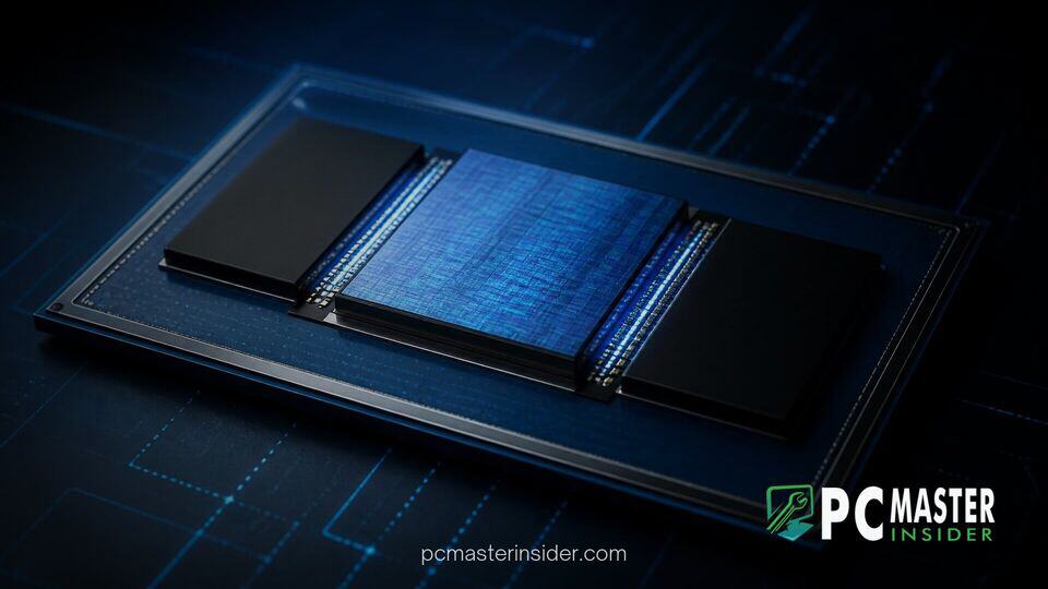
EMIB technology uses die-level silicon bridges embedded within the substrate to connect multiple distinct chiplets with high speed, low latency interconnects. This heterogeneous approach enables chip architects to mix and match compute, memory, and acceleration components from different manufacturing nodes inside a single compact package. The contract provides Intel with a flagship customer for its advanced packaging services, validating its strategy to monetize packaging independently from front end wafer fabrication.
The multi-year agreement also secures long term supply capacity for Intel Xeon processors within Azure data centers, including future deployments based on the upcoming Diamond Rapids microarchitecture. Beyond raw hardware delivery, the two companies will collaborate closely on optimizing system level capabilities, ranging from Compute Express Link memory pools to hardware accelerated hardware security features.
Impact on Custom Azure Silicon and Enterprise Hardware
Microsoft's adoption of EMIB packaging comes as cloud providers accelerate the development of proprietary chips tailored for artificial intelligence and cloud computing. Heterogeneous multi-chiplet designs allow hyperscalers to scale compute power efficiently while controlling power budgets. By pairing Microsoft's custom architecture with Intel's packaging capabilities, Azure aims to deliver tailored hardware optimizations for complex enterprise workloads.
The partnership spans multiple enterprise computing layers, touching on confidential computing, virtual machine performance, and hardware acceleration. Microsoft is actively building out advanced infrastructure capabilities across Windows and cloud platforms, ranging from hybrid developer integrations like GitHub Copilot local model routing to OS security enhancements like user mode endpoint security architecture. Deep hardware integration with Intel's Xeon platform ensures enterprise cloud instances receive tailored optimizations for database operations and encrypted virtualization.
For the broader semiconductor market, Intel's ability to secure a major customer like Microsoft for advanced packaging serves as proof of concept for its foundry business model. While contract wafer manufacturing remains highly competitive, packaging services offer a high demand entry point for cloud giants seeking flexible chiplet integration.
With 18A yields reaching stable commercial thresholds and high profile partners committing to its advanced packaging ecosystem, Intel has taken an important step in proving its manufacturing capabilities. As Microsoft begins integrating EMIB connected silicon into its Azure data centers, both companies stand to gain from deeper system level hardware co-engineering.