
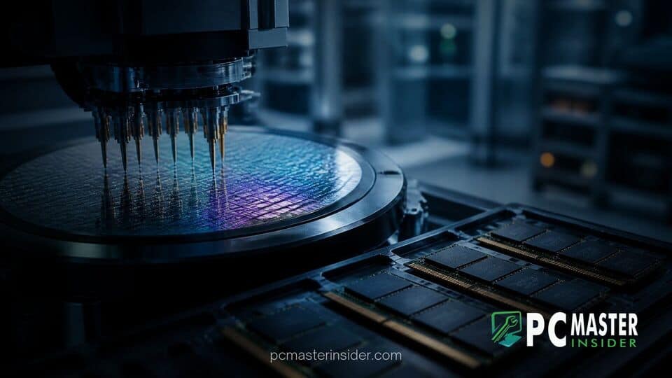
China's leading dynamic random-access memory (DRAM) manufacturer, ChangXin Memory Technologies (CXMT), is executing a substantial capital deployment aimed at expanding its in-house backend testing infrastructure and scaling up overall output . Utilizing over-raised capital from its recent initial public offering, the chipmaker is allocating billions of yuan toward advanced research and the second phase of its memory wafer testing base in Hefei .
By bringing a larger proportion of its wafer inspection, module assembly, and quality assurance processes in-house, CXMT aims to mitigate third-party packaging constraints . The initiative comes at a vital juncture for the global technology ecosystem, where rapid adoption of enterprise AI and personal computing hardware has created an ongoing squeeze on worldwide memory availability.
CXMT Expands Capital Investment for DRAM Testing Infrastructure
To prevent downstream production bottlenecks as wafer output scales, CXMT is directing 18 billion Chinese yuan from its surplus IPO proceeds into a broader 34.9 billion yuan investment framework . This strategic move strengthens the company's position as a full-fledged Integrated Device Manufacturer (IDM), unifying circuit design, front-end fabrication, and backend assembly .
According to official disclosures, the funding will be split between equipment-heavy R&D initiatives and dedicated physical testing facilities . The expansion addresses a growing operational reality: as front-end semiconductor fabrication capacity ramps up, relying solely on outsourced assembly and test (OSAT) vendors risks creating severe operational lag. By internalizing these services, CXMT intends to streamline unit testing, improve chip yield efficiency, and lower overall production costs .
Phase II Backend Testing Expansion and Production Details
The backend expansion relies heavily on a 10.8 billion yuan project dedicated to the Phase II construction of the memory wafer testing base operated by subsidiary ChangXin Storage Products (Hefei) Co., Ltd . Supported directly by 5 billion yuan in capital injection and shareholder loans from the parent entity, this site will house specialized equipment for high-throughput memory inspection, validation, and component packaging .
The remaining capital portion, amounting to 13 billion yuan from surplus IPO funds, will feed into a 24.1 billion yuan 12-inch memory wafer technology R&D project spanning 30 months in Hefei . Over 92 percent of the budget for the R&D initiative is designated for advanced silicon processing and analysis equipment . This ensures that as CXMT pushes for higher density architectures, its testing tools keep pace with the strict reliability requirements demanded by consumer electronics and enterprise platforms.
Addressing Global Memory Constraints and Consumer PC Market Impact
CXMT's investment in backend throughput arrives at a critical juncture for the broader electronics industry. Top-tier memory manufacturers like Samsung have seen revenue surge as global average selling prices rise, largely driven by enterprise data centers soaking up vast quantities of high-bandwidth memory. This strategic shift by primary producers toward high-margin AI servers has left consumer-grade DDR4 and DDR5 inventory increasingly tight.
The broader impact of these pricing realities has already trickled down to consumer hardware. Industry executives like Team Group's CEO have warned of memory shortages extending well into coming cycles. Higher component pricing has also directly affected hardware configurations, as shown by recent data where high-capacity RAM adoption has slowed among system builders due to elevated retail costs.
By solidifying its internal testing pipelines, CXMT is working to keep its volume production lines running at high efficiency. Increased yield rates and faster validation cycles mean the firm can pump more reliable standard DRAM modules into mainstream market channels, offering relief to desktop and mobile system integrators seeking stable supply.
Future Fabs and Technological Milestones for CXMT
Alongside its expanded backend infrastructure, CXMT continues to advance its process node capabilities . The company has made notable strides with its fifth-generation DRAM technology platform, utilizing multi-patterning techniques to push structural feature sizes down to sub-12 nanometers . This platform enables up to a 50 percent increase in functional memory dies per wafer, significantly boosting overall production efficiency .
Furthermore, CXMT is exploring next-generation 4F² transistor architectures aimed at server-class DDR5 applications, designed to increase storage density while navigating lithography constraints . Operating software environments are adapting simultaneously; for instance, modern operating systems have evolved through updates where Windows 11 optimized system memory efficiency to maintain responsiveness across constrained hardware configurations.
As CXMT completes its multi-year facility buildout in Anhui Province, its integrated manufacturing model will play an influential role in shaping memory market dynamics . By securing both front-end R&D and backend testing capacity internally, the chipmaker positions itself to deliver a steady volume of DRAM products to global technology markets .